Industries We Enable
Kaynes Semicon supports semiconductor programs across industries where reliability, performance, and production scale are critical.


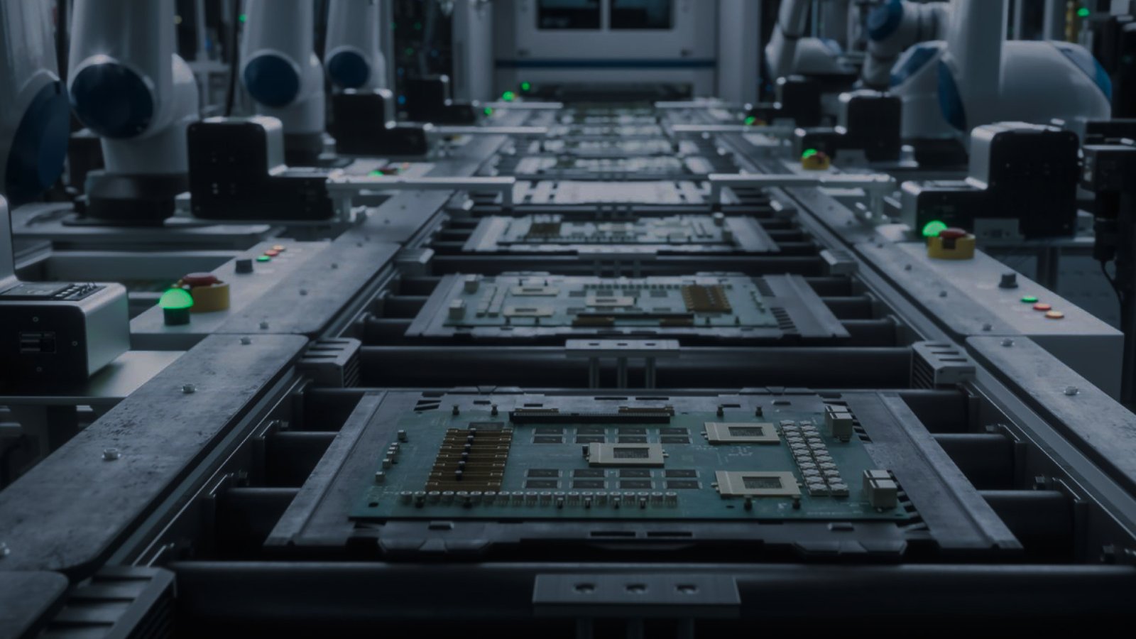
India’s Semiconductor Backend Platform
Kaynes Semicon is establishing India’s semiconductor backend manufacturing platform — integrating assembly, packaging, reliability engineering, and test infrastructure required for industrial-scale semiconductor programs.

Engineering Domains
Kaynes Semicon operates across specialised engineering domains that support semiconductor products from device integration through qualification and production release.
Platform Execution Highlights
The semiconductor platform is supported by execution capabilities spanning manufacturing infrastructure, supplier networks, and global program coordination.

Partnerships across global semiconductor technology ecosystems

Integrated packaging, test engineering, and reliability
capability

Supplier network across semiconductor materials and equipment

Logistics infrastructure supporting global semiconductor
programs

Platform readiness for power semiconductor and industrial electronics programs


Anchored in India’s Semiconductor & ESDM Mission
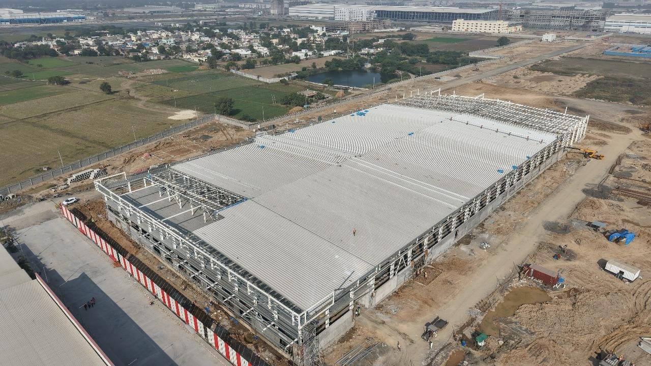
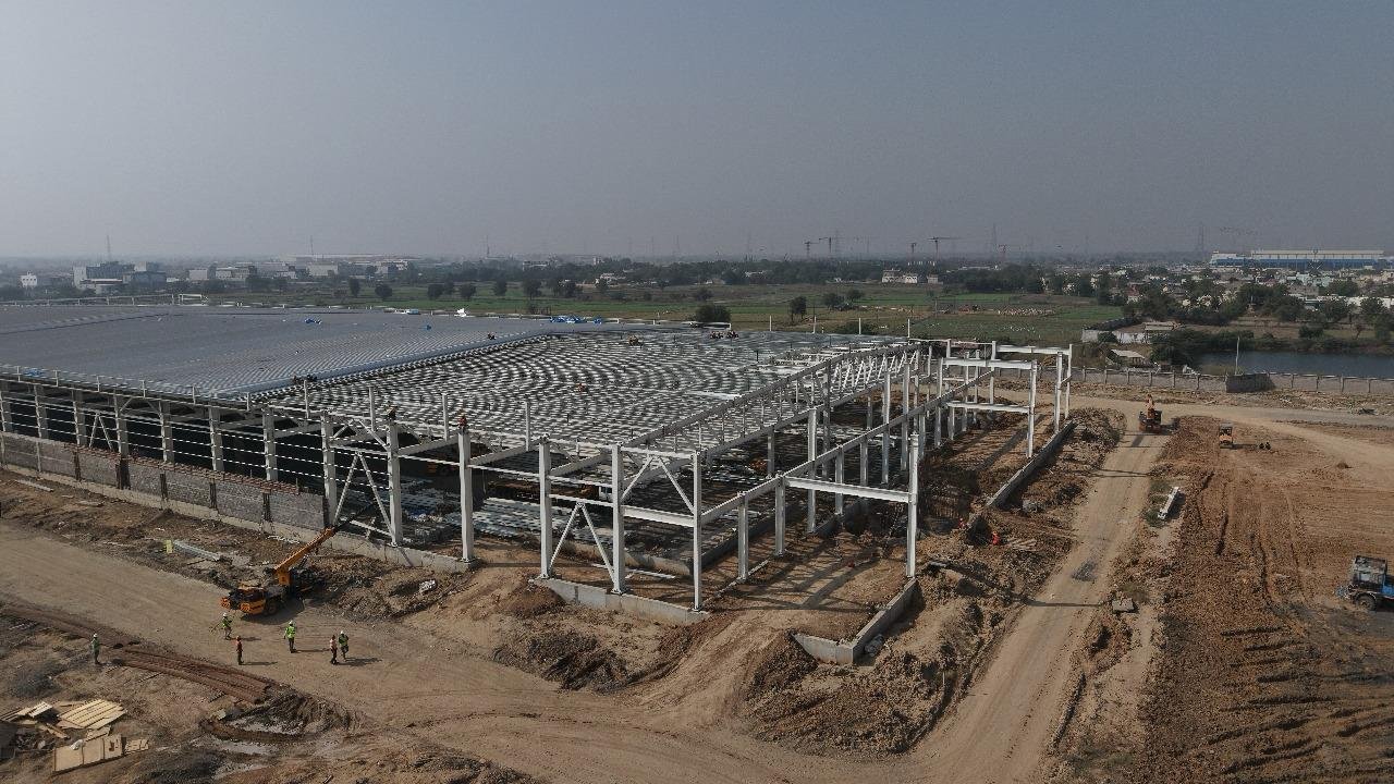
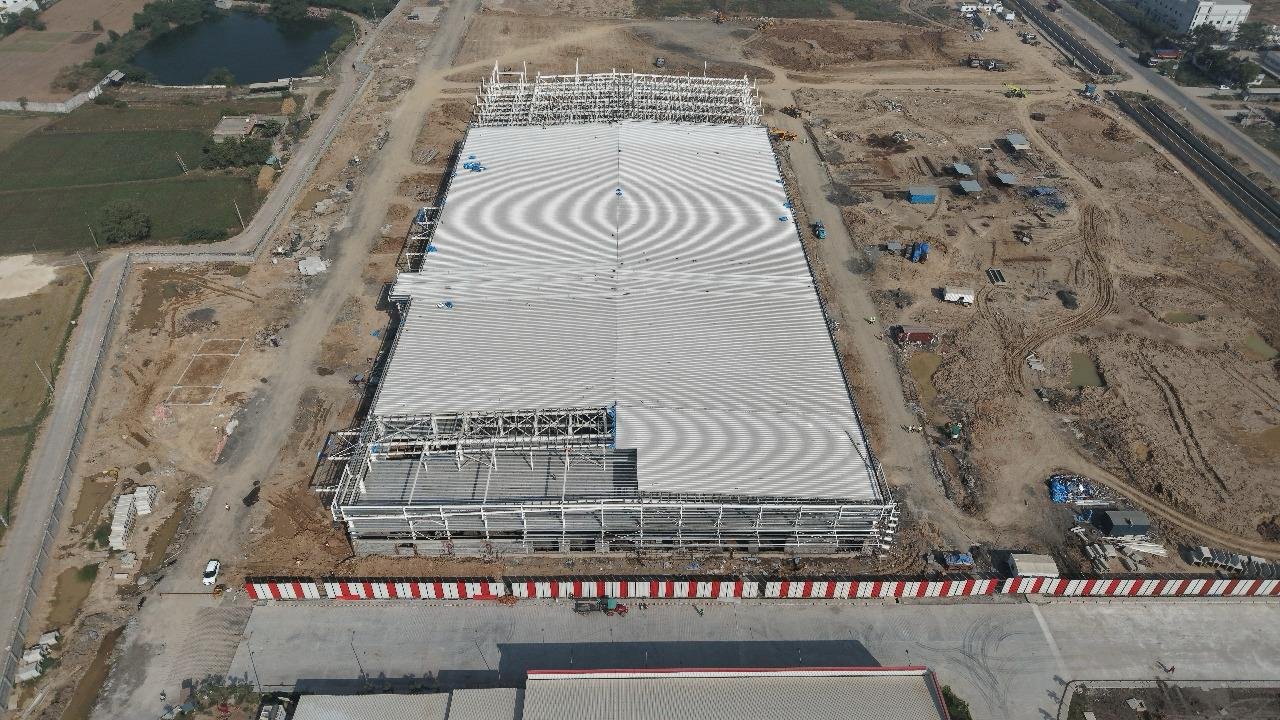
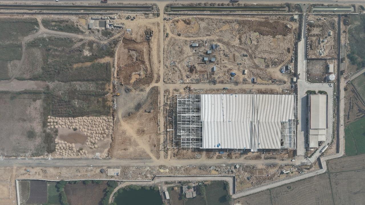
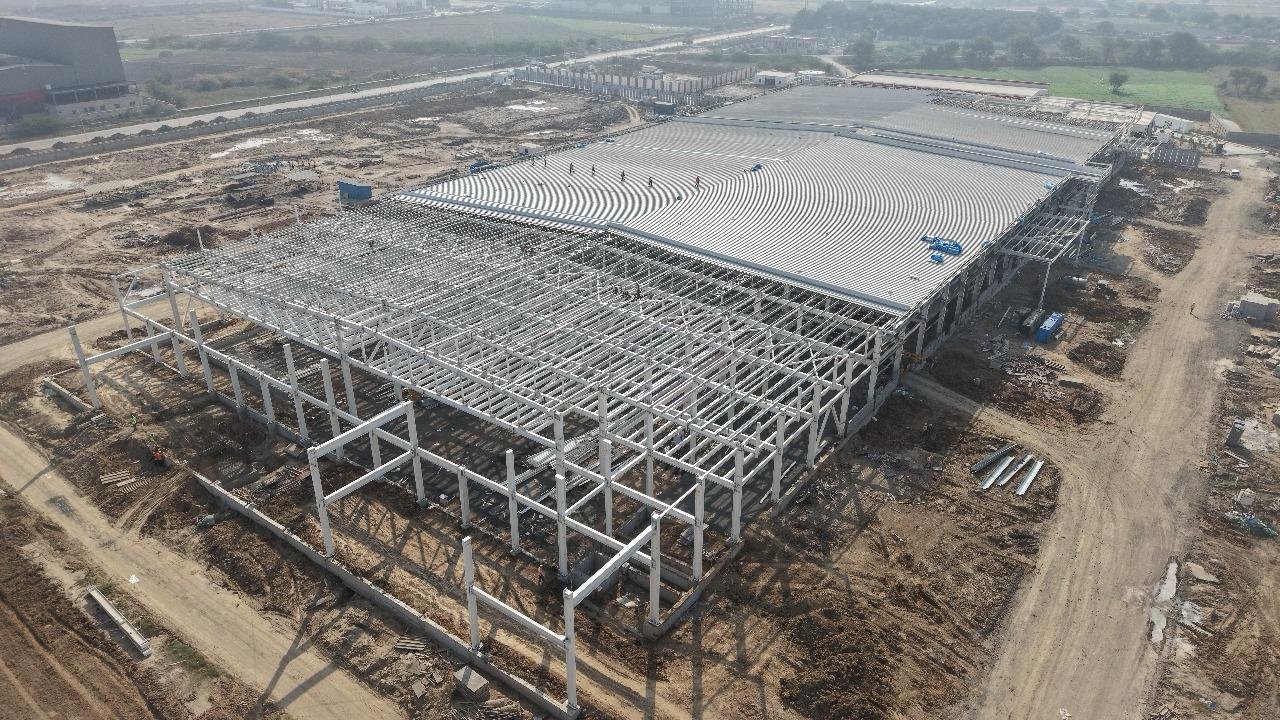
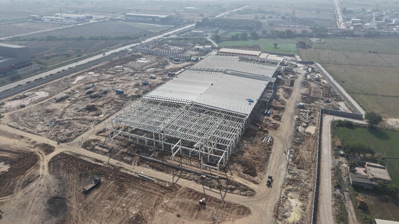
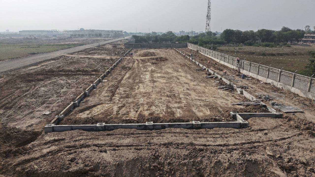
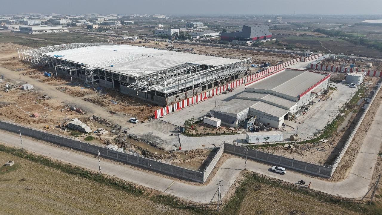
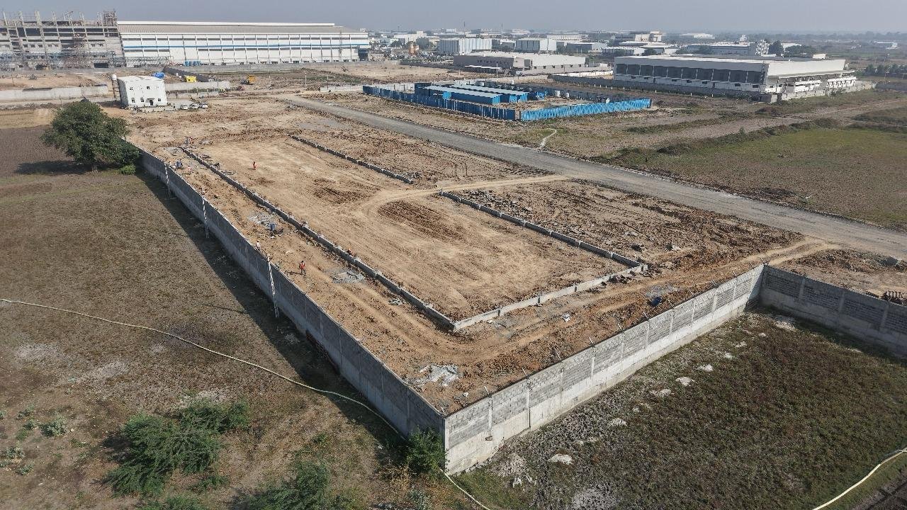
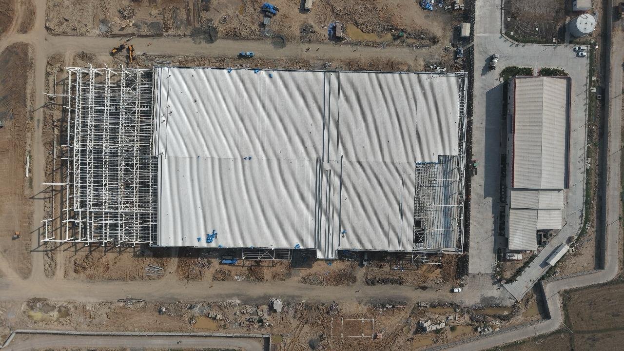
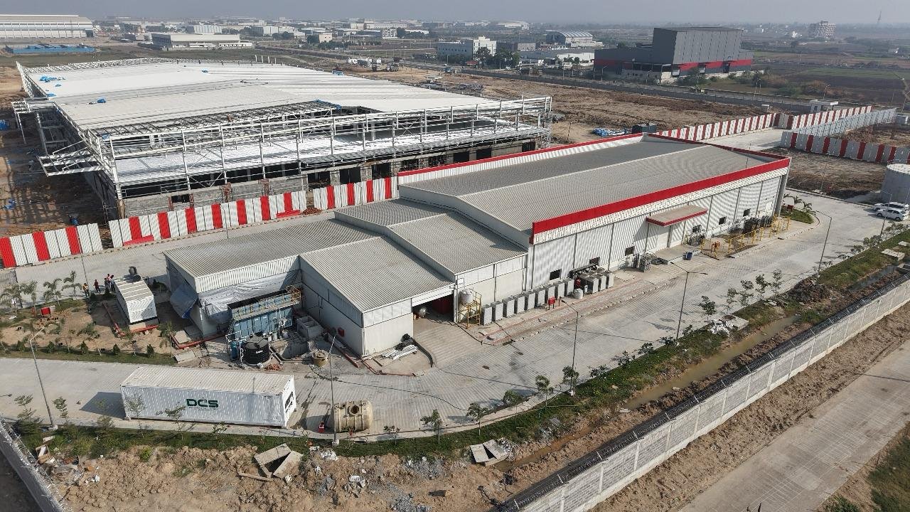
Sanand Semiconductor OSAT Platform — Gujarat, India Kaynes Semicon is building a phased semiconductor assembly and test platform designed to support industrial-scale manufacturing. 1,200 sq m operational pilot OSAT facility 19,000+ sq m semiconductor cleanroom infrastructure under development Structured across three units enabling progressive manufacturing scale.


Semiconductor Ecosystem
Semiconductor manufacturing platforms are built through coordinated collaboration across technology providers, materials suppliers, academic institutions, and logistics infrastructure.
Kaynes Semicon operates within a growing semiconductor ecosystem that supports engineering development, manufacturing readiness, and global program execution.

Certification
ISO 9001
Quality Management Systems
IATF 16949
Automotive Quality Management
ISO 14001
Environmental Management Systems
ISO 45001
Occupational Health & Safety Management
Experience Anchored in Accountability
Our leadership team brings deep experience across semiconductor manufacturing, reliability, and industrial engineering. We believe institutions are built through discipline, governance, and sustained commitment — not acceleration alone.
Aatmanirbhar Bharat Abhiyan (Make In India)
Semiconductor capability is built through coordinated collaboration across technology partners, materials suppliers, equipment providers, and manufacturing ecosystems. Kaynes Semicon operates within India’s emerging semiconductor ecosystem supporting packaging innovation, supply chain resilience, and manufacturing scale. Facility development aligns with national semiconductor initiatives and the Gujarat Semiconductor Policy (GSEM).

The Leadership Lens
Kaynes Semicon is led by a team with experience across semiconductor engineering, electronics manufacturing, and industrial technology development. Leadership expertise spans packaging technologies, semiconductor systems, manufacturing operations, and global electronics supply chains.
Learning from Practice
We share perspectives shaped by real execution — technical progress, operational milestones, and industry developments across semiconductor manufacturing and ecosystem development.
India’s Semiconductor Surge: How Kaynes Semicon is Powering the Nation’s Chipmaking Ambitions
India’s Semiconductor Surge: How Kaynes Semicon is Powering the Nation’s Chipmaking Ambitions

India’s Semiconductor Ambition: Kaynes Semicon Leading the OSAT Wave
India’s Semiconductor Ambition: Kaynes Semicon Leading the OSAT Wave
Semiconductor Industry Set to Cross USD 950 B by 2030, Driven AI, 5G, and IoT.
