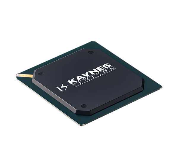
FCBGA packages use flip-chip bonding to mount the die face-down directly onto a substrate, minimizing the length of interconnects and significantly improving speed and power handling. This structure is ideal for performance-intensive applications such as AI processors, GPUs, networking ASICs, and enterprise-grade computing.
Advantages of FCBGA package

Short Electrical Paths
Direct die-to-substrate connections enhance speed.

Excellent Signal Integrity
Supports high-frequency operation with minimal loss.

Efficient Power Delivery
Optimized for high-current, low-resistance paths.

Advanced Thermal Dissipation
Controlled impedance pathways lower signal interference.

Higher Integration Density
Enables integration of multiple dies or components.

Greater I/O Capability
Supports extremely high pin counts.

Supports Large Die Sizes
Ideal for AI, HPC, and server-class processors.

Reduced Package Warpage
Stable during assembly and operation.

Customizable Substrate Design
Supports routing complexity and embedded passives.

Robust Mechanical Strength
Withstands thermal and mechanical stress.

Compatible with Advanced Nodes
Suitable for advanced FinFET and EUV-based chips.

Scalable for 2.5D Integration
Can support interposers or stacked memory chips.